Chip manufacturing technology
Q5: What is the formula for calculating wafer roughness?
There are various methods to represent surface roughness. Here are three of the most common surface roughness parameters, along with their definitions and formulas. Common surface roughness parameters:
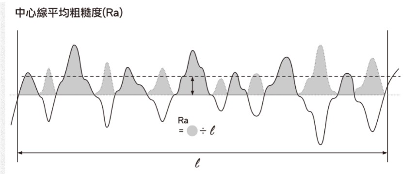
1.Ra: Arithmetic Average Roughness
Ra is calculated by measuring the deviations of the surface profile from the mean line within a specified length L. The formula for Ra is the sum of the absolute values of these deviations divided by the measuring length L, with the centerline serving as the X-axis within the measured length L.

formula:Ra=|f(x)|dx / l
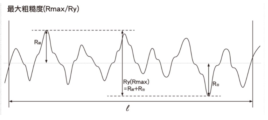
2.Rmax[CNS]=Ry[JIS]:Maximum Roughness
Rmax[CNS] and Ry[JIS] represent the maximum roughness of the surface. It is measured as the vertical distance between the highest peak and the lowest valley within a specified length L along the surface profile curve. Rmax and Ry follow the same algorithm conceptually, but they differ in the selection of peaks and valleys. In recent years, Ry has largely replaced Rmax.

formula:Rmax=Ry=Rp+Rv
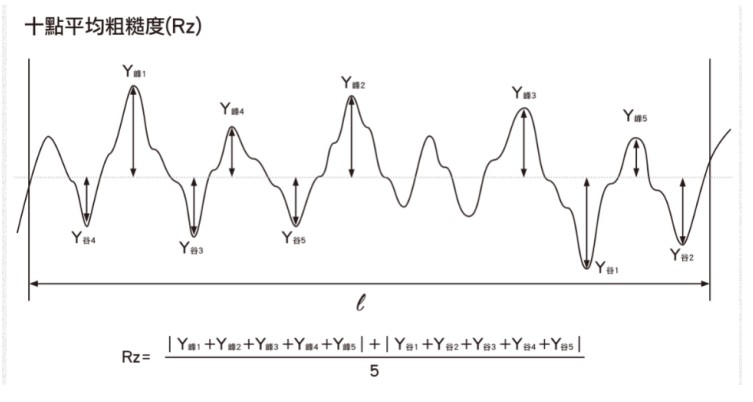
3.Rz: Ten-point Mean Roughness
Rz represents the ten-point mean roughness of the surface. It is calculated as the average of the absolute values of the vertical distances between the five highest peaks and the five lowest valleys within a specified length L along the surface profile curve.

The relationship between center-line average roughness (Ra), maximum roughness (Ry), and ten-point average roughness (Rz) is approximately 4Ra ≈ Ry ≈ Rz, and their units are all in micrometers (µm).
Q6: Please introduce what TSV and XRD are.
Definition:
- TSV (Through-Silicon Via):
TSV is a technology that enables holes to pass through the entire chip, allowing vertical connections between different layers or regions. TSV technology is commonly used in the manufacturing of 3D ICs (Three-Dimensional Integrated Circuits) to achieve higher integration and performance.
- XRD (X-ray Diffraction):
XRD is a technique used to analyze material crystal structures and crystalline properties. It utilizes the interaction between X-rays and the crystal structure to deduce information such as material crystal structure, lattice parameters, and crystal size. XRD technology is commonly used to analyze the crystal structures and quality of different regions on chips to ensure process accuracy and product quality.
Comparison:
- Application Areas:
TSV technology is primarily applied in the semiconductor manufacturing field to achieve electrical interconnections or energy transfer between different layers or regions within the chip. XRD technology is mainly applied in the fields of materials science and analysis to analyze material crystal structures, lattice parameters, and crystalline quality. Functions and Purposes:
The main function of TSV technology is to realize vertical connections within the chip to enhance chip integration and performance. The main function of XRD technology is to analyze material crystal structures and quality to understand material crystalline characteristics, crystallographic phases, and defect situations. Operation Modes:
TSV technology typically involves processing and manufacturing silicon wafers, including steps such as etching holes and filling conductor materials. XRD technology involves irradiating materials with X-rays and measuring the scattering patterns and intensities of X-rays to deduce material crystal structures and crystalline characteristics. Expertise and Equipment:
TSV technology requires expertise in microfabrication and semiconductor processing, along with the use of corresponding manufacturing equipment. XRD technology requires expertise in materials analysis and crystallography, along with the use of X-ray analysis instruments for experimentation.
Q7: What is the relationship between white light interferometry and surface roughness of chips?
"White Light Interferometry" (White Light Interferometry) and "surface roughness" are two concepts commonly discussed in materials science and engineering, rather than a single chip technology. However, there is indeed some relationship between them, especially in assessing the surface quality and characteristics of chips.
White Light Interferometry:
White light interferometry is a non-contact optical technique used to measure surface morphology and film thickness. It utilizes the principle of optical interference to measure the surface roughness and film thickness by observing the interference effects of light reflected from the surface.
White light interferometry instruments typically include a white light source and an interferometer, which can generate high-resolution surface contour images and film thickness distributions.
Surface Roughness:
Surface roughness refers to the irregularity and roughness of a surface, usually referring to its microscopic characteristics. It can be assessed through various methods, including optical, surface morphology analysis, and atomic force microscopy techniques.
Surface roughness is an important performance indicator for many applications. For example, in chip manufacturing, surface roughness may affect the performance and functionality of chips.
Correlation:
During chip manufacturing processes, white light interferometry can be used to assess the morphology and flatness of chip surfaces, as well as to measure surface roughness.
By using white light interferometry instruments, manufacturers can rapidly and accurately assess the surface roughness of chips, thereby ensuring process accuracy and product quality.
In summary, white light interferometry and surface roughness are concepts closely related to chip manufacturing and quality control. They can complement each other to ensure the flatness and performance of chip surfaces.
Q8: What is the relationship between AFM and surface roughness of chips?
Atomic Force Microscopy (AFM) is a high-resolution surface morphology imaging technique that can be used to measure the roughness of chip surfaces. AFM has significant applications in studying the surface roughness of chips. Here's the relationship between them:
1. High-resolution imaging: AFM can provide surface morphology images at the sub-nanometer level, accurately displaying the microstructures and morphology of chip surfaces, including surface roughness.
2. Surface topography analysis: AFM can scan the chip surface at the atomic scale and measure the height variations of the surface based on the movement of the probe. This allows quantification of the surface roughness of chips and provides detailed information about surface topography.
3. Surface roughness measurement: AFM can directly measure roughness parameters of chip surfaces such as Root Mean Square (RMS), Average Roughness (Ra), etc. These parameters offer a quantitative assessment of chip surface roughness.
4. Material property analysis: Besides surface morphology, AFM can also be used to study other material properties of chip surfaces such as hardness, elasticity, etc., which are closely related to chip surface roughness.
5. Processing quality control: During chip manufacturing processes, AFM can serve as a quality control tool to inspect the surface roughness during processing, ensuring that the final product meets quality requirements.
Therefore, AFM is a highly useful tool for studying and measuring the roughness of chip surfaces, providing essential support for surface quality control in semiconductor manufacturing and other fields.