Optical detection technology
Q1: What are the testing technologies for wafers?
1. Optical Inspection:
• Microscopic Inspection: Observing the surface of the wafer with a microscope to detect defects or foreign particles.
• Reflectance Measurement: Detecting surface or film issues by measuring the reflectance of light.
2. Electron Beam Inspection:
• Scanning Electron Microscope (SEM): Scanning the surface of the wafer with an electron beam to provide high-resolution images for detecting minute defects.
• Transmission Electron Microscope (TEM): Detecting the microstructural features of crystals and films.
3. X-ray Inspection:
• X-ray Imaging: Detecting crystal quality and structure by irradiating the wafer with X-rays and recording their interaction with the wafer.
4. Electrical Testing Techniques:
• Resistance Testing: Measuring the resistance of different areas on the wafer to detect possible electronic device failures.
• Capacitance Testing: Evaluating the performance of electronic components on the wafer by measuring capacitance.
5. Chemical Analysis:
• Mass Spectrometry: Analyzing the elemental composition of the wafer surface using a mass spectrometer to detect potential contamination or impurities.
• Raman Spectroscopy: Analyzing the chemical composition of the wafer surface by utilizing the frequency changes of scattered light with a laser light source.
6. Thermal Testing:
• Thermal Microscope: Detecting defects or structural issues by observing the thermal response of the wafer at different temperatures.
7. Mechanical Testing:
• Hardness Testing: Evaluating the strength and durability of the wafer's structure by measuring the surface hardness.
Q2:What techniques are used to inspect wafer flatness?
To assess the flatness of a wafer, optical and mechanical measurement techniques are commonly employed. Here are some common methods:
1. Surface Profiler: This is a commonly used mechanical measurement device that measures the height and contour of the wafer surface. By moving a sensor and recording changes in surface height, surface topography maps can be generated to assess flatness.
2. Laser Interferometer: Using laser interferometry, surface height variations are detected by measuring the interference patterns of laser beams. This provides high-resolution and precise surface height information.
3. White Light Interferometer: This device utilizes the principle of white light interferometry to determine variations in surface height by measuring interference of light, which can be used to detect wafer surface flatness.
4. Microscopic Inspection: Microscopes are used to observe the wafer surface, particularly at the edges and other critical areas, to detect potential irregularities or unevenness.
5. Capacitive Sensing: Capacitive sensors measure changes in capacitance on the wafer surface, as variations in surface flatness affect capacitance values.
6. Raman Microscopy: Although typically used for chemical analysis, Raman microscopy can also be used to observe microstructural features of the wafer surface, thereby detecting flatness issues.
These techniques can be used individually or in combination, depending on the range of flatness to be inspected, the precision requirements, and the practical conditions during the manufacturing process. Ensuring wafer flatness is crucial for subsequent process steps and device performance in semiconductor manufacturing.
Q3: How to test electrical wire characteristics (ESD - Electrostatic Discharge Testing)
ESD testing typically involves measuring the response of a device in a static discharge environment to assess its sensitivity to electrostatic discharge. The steps may include:
1. Setting test conditions: Establishing the conditions for electrostatic discharge testing, including parameters such as discharge current, voltage, etc.
2. Testing the sample: Placing the device or electrical wire to be tested in an environment simulating an ESD event.
3. Recording responses: Monitoring the response of the testing equipment, such as voltage, current, performance changes, etc.
4. Analyzing results: Assessing the device's resistance to ESD based on the test outcomes.
This type of testing is commonly employed in the manufacturing of electronic devices to ensure that they are less susceptible to damage from electrostatic discharge during actual use.
Q4: What does the final test in chip testing include?
The final test in chip manufacturing, conducted after chip packaging, but before delivery to end-users, is a crucial step to ensure chip functionality and performance. Its objective is to validate whether the chip meets design specifications and functions correctly. Here's what a typical final test includes:
1. Electrical Performance Testing:
• Voltage Testing: Measure chip performance under different voltage conditions.
• Current Testing: Measure chip performance under different current loads.
2. Logic Functionality Testing:
• Logic Function Verification: Ensure the chip's logic circuits operate as per design specifications.
• Timing Tests: Assess chip timing performance, including clock frequency and signal propagation delays.
3. Communication Interface Testing:
• Protocol Testing: If the chip has communication interfaces, test if they comply with relevant communication protocols like I2C, SPI, UART, etc.
• Data Transmission Testing: Assess chip performance in data transmission.
4. Analog Circuit Testing:
• Analog Circuit Performance Testing: If the chip contains analog circuits like amplifiers, filters, etc., test their performance.
5. Memory Testing:
• RAM Testing: Ensure random-access memory operates correctly.
• ROM/Flash Testing: Verify the functionality of non-volatile memory for writing and reading operations.
6. Power Consumption Testing:
• Static Power Testing: Test chip static power consumption in different modes.
• Dynamic Power Testing: Test chip dynamic power consumption under different workloads.
7. Temperature Characteristics Testing:
• Temperature Range Testing: Assess chip performance under various temperature conditions.
8. Reliability Testing:
• Long-Term Operation Testing: Run the chip for an extended period to detect issues arising from prolonged use.
• Temperature Cycling Testing: Conduct cycling tests at different temperatures to evaluate chip temperature stability.
9. External Interface Testing:
• Pin and Connector Testing: Test the connectivity and reliability of chip external pins and connectors.
10. Packaging Testing:
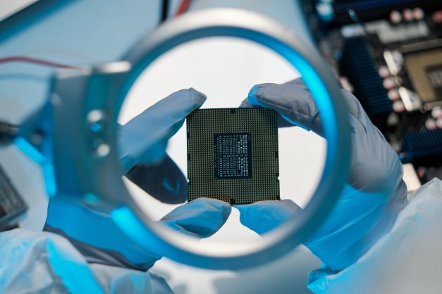
• Visual Inspection: Inspect the packaging for integrity, cracks, or damage.
• Pin Soldering Testing: Check the quality of pin soldering on the package.
Surface Reflection Detection:
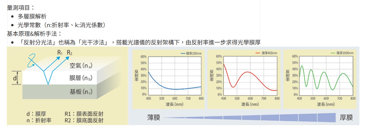
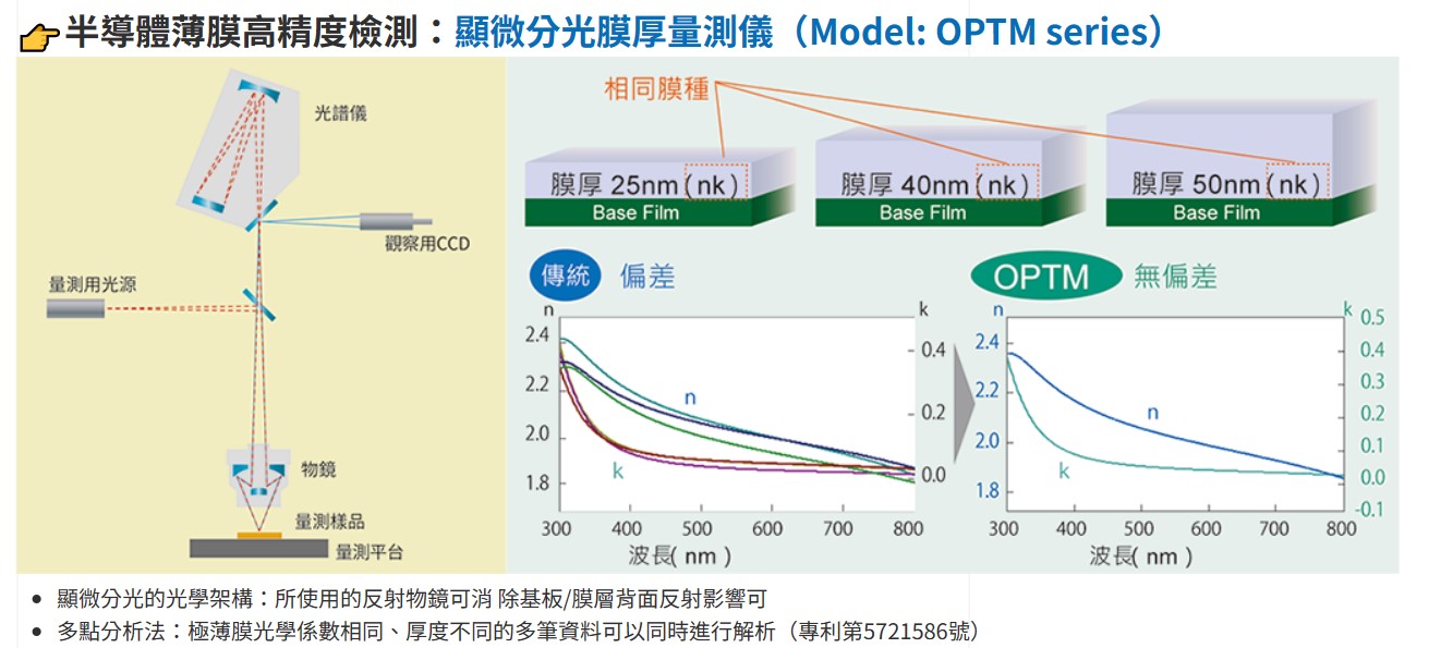
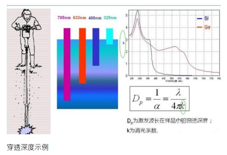
Using a beam of light to illuminate the surface of a wafer, observing the characteristics of the reflected light to detect surface defects or contamination.
Transmissive light inspection:
By passing a light source through transparent wafer materials, observing the characteristics of the transmitted light to detect material uniformity and internal defects
Interferometric inspection:
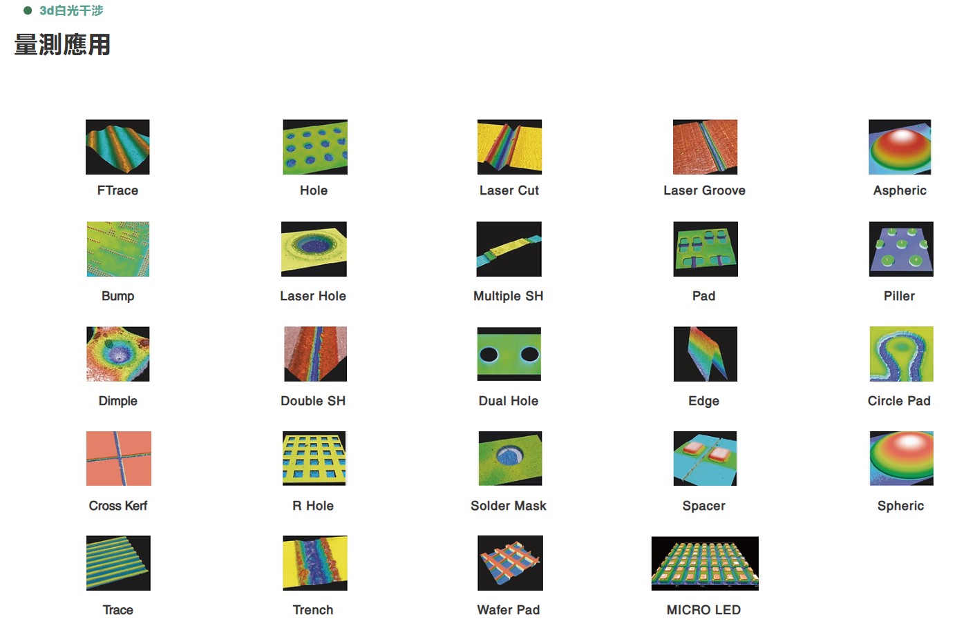
Utilizing interference effects such as phase differences and interference fringes to detect the flatness and thickness variations of the wafer surface.
Near-infrared inspection:
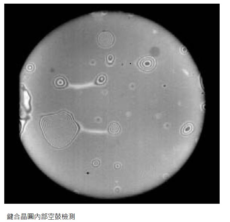
Utilizing a near-infrared light source with a wavelength of around 1100 nanometers, passing through the wafer to detect internal features. Near-infrared light, with its superior penetrative properties, is employed to observe internal structures, aiding in ensuring chip quality.
X-ray diffraction analysis:
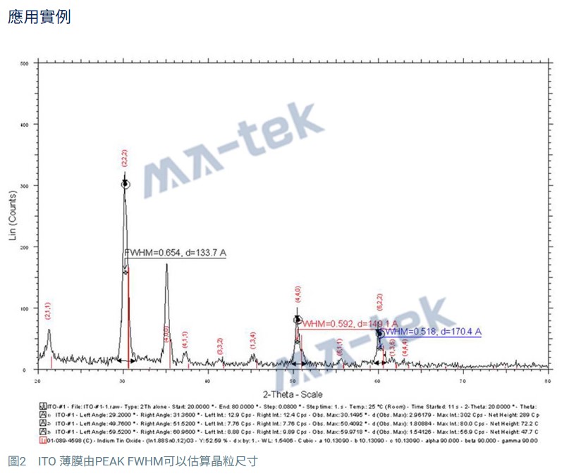
X-ray diffraction (XRD) is primarily used for macroscopic analysis of crystal structures but can also be applied to analyze the stacking structure and film characteristics of wafers. It provides information about the internal structure of the wafer without the need for sample destruction.
Analysis Applications:
1. Triple Crystal High-Resolution X-ray Diffraction (HRXRD)
2. Crystallinity Analysis
3. Grain Size Analysis
4. X-ray Reflectivity (XRR) Analysis of Multilayer Film Thickness, Roughness, and Density
5. Concentration Analysis of Compound Films
6. Grazing Incidence Diffraction (GID) Analysis of Thin Films at Low Angles
7. Powder X-ray Diffraction (Powder XRD) Analysis
8. Crystal Structure and Phase Identification
9. Lattice Parameter Analysis
10. Identification of Oxidation, Corrosion, and Thin Film Coatings
11. Reciprocal Space Mapping (RSM) Analysis
12. Epitaxial Growth Analysis
